





human + AI workflows
The New Frontier: Elevating AI-Assisted PCB Design for KiCad 10
The New Frontier: Elevating AI-Assisted PCB Design for KiCad 10 The landscape of hardware engineering is undergoing a profound transformation, driven by the integration of artifici
The New Frontier: Elevating AI-Assisted PCB Design for KiCad 10
The landscape of hardware engineering is undergoing a profound transformation, driven by the integration of artificial intelligence into critical design workflows. For users of KiCad 10, this evolution is particularly impactful, as AI-assisted PCB design for KiCad 10 is rapidly moving from theoretical concept to practical application. This shift promises to enhance efficiency, accuracy, and innovation in creating complex electronic circuits, fundamentally reshaping how engineers approach their projects. As AI agents become increasingly capable, the synergy between human expertise and machine intelligence is unlocking unprecedented possibilities in the realm of PCB development.
01What is AI-Assisted PCB Design in KiCad 10?
AI-assisted PCB design in KiCad 10 refers to the integration of artificial intelligence tools and plugins that augment the capabilities of the popular open-source electronic design automation (EDA) suite. These solutions leverage large language models (LLMs) and specialized algorithms to automate, optimize, and validate various stages of the PCB design process. Rather than replacing human designers, AI acts as an intelligent copilot, streamlining tasks and offering insights that accelerate development cycles.
Want your team to run this workflow with AI-native execution?
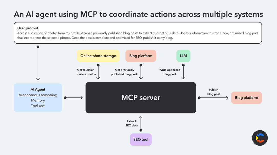
Central to this advancement are native KiCad plugins, such as mixelpixx/Konnect, which functions as a single Rust binary. Konnect exposes a comprehensive suite of 217 schematic, layout, routing, placement, design-review, and manufacturing tools to AI assistants like Claude, utilizing a Model Context Protocol (MCP). This allows AI agents to interact directly with KiCad's functionalities, enabling them to assist with complex operations.
Another notable example is the KiCad AI Assistant, an LLM-powered plugin designed to understand and execute commands given in plain English. Similarly, the ALT TAB Circuit Copilot offers an in-editor chatbot and assistant for schematic and PCB design. These tools empower designers to articulate their requirements conversationally, allowing the AI to translate natural language into design actions within the KiCad environment.
The capabilities of these AI-assisted tools span the entire PCB design lifecycle. They can facilitate schematic capture, automate PCB layout and routing, perform Electrical Rule Checks (ERC) and Design Rule Checks (DRC), conduct comprehensive design-review audits, and even assist with tasks like JLCPCB part searches and the generation of reference circuits. Furthermore, they can manage a full manufacturing export pipeline, often equipped with bundled skills and agents pre-trained on KiCad conventions, ensuring adherence to best practices right out of the box.
02Why Embrace AI for KiCad 10 PCB Design?
The adoption of AI in KiCad 10 PCB design is driven by a compelling set of benefits that address the growing complexities and demands of modern electronics development. The primary motivations revolve around enhancing efficiency, managing intricate designs, ensuring precision, and making advanced design capabilities more accessible.
One of the most significant advantages is the dramatic increase in efficiency. AI agents can automate repetitive and time-consuming tasks, freeing human engineers to focus on higher-level problem-solving and innovation. This automation extends to various aspects, from initial schematic drafting to final manufacturing preparations, significantly shortening design cycles.
AI also proves invaluable in managing the complexity of modern PCBs. Engineers have successfully used AI to help build PCBs with over 150 components, demonstrating its capability to handle intricate designs that would otherwise require extensive manual effort. This success is not limited to simple tasks but extends to complex board layouts and routing challenges.
Precision and validation are further enhanced through AI integration. The development of AI-generated circuit boards emphasizes the need for deterministic writers, machine-readable validation, and honest stop conditions. These features ensure that AI-assisted designs are not only functional but also adhere to stringent quality and safety standards, minimizing errors and rework.
Accessibility is another key benefit. With LLM-powered plugins, designers can interact with KiCad using plain English commands. This simplifies schematic editing, allowing users to place symbols, set properties, draw wires, connect pins, and manage hierarchical sheets merely by asking. This intuitive interaction lowers the barrier to entry for complex design tasks and accelerates the workflow for experienced users.
Moreover, AI can significantly improve design checks. The ability to integrate AI with KiCad 10 for design checks ensures that critical aspects are not overlooked. AI assistants can perform thorough audits, identifying potential issues or forgotten elements that might escape human review, thereby bolstering the reliability and robustness of the final product. This
capability is especially valuable when a project involves multiple power domains, high-speed interfaces, or strict manufacturing constraints.
03Core Workflows AI Can Improve
Schematic creation and documentation
A typical AI-assisted workflow begins with a structured design brief. Instead of asking an assistant to “make a board,” provide the intended function, supply voltages, interfaces, component constraints, and safety requirements. For example:
Create a 5 V-to-3.3 V sensor interface with USB-C power input, reverse-polarity protection, an indicator LED, an I²C header, and test points for both rails.
An assistant can use this information to propose a block diagram, identify likely circuit sections, and suggest commonly used components. It may then help place symbols, assign values, connect nets, and organize the design into hierarchical sheets.
The human designer must still verify every important electrical decision. AI can recommend a regulator, but it may not know the required output current, thermal environment, switching-frequency restrictions, or availability requirements unless those constraints are explicitly supplied. It can also confuse similarly named pins or overlook manufacturer-specific layout guidance. The most reliable approach is to treat generated circuitry as a draft that must be checked against datasheets and the project specification.
AI is also useful for documentation. It can generate net labels, connector descriptions, signal summaries, and design notes in a consistent format. Clear labels such as +3V3_SENSOR, USB_VBUS, and I2C_SDA are easier to review than automatically generated names such as Net-(U1-Pad3). Well-documented schematics improve collaboration and make later debugging significantly easier.
Symbol and footprint selection
Component selection is often one of the most tedious parts of PCB design. An AI assistant can narrow a search based on package, voltage rating, current capability, tolerance, operating temperature, and distributor availability. It can also compare alternatives and flag mismatches between a schematic symbol and the selected footprint.
However, database information can be incomplete or outdated. Before committing a part, verify the manufacturer part number, lifecycle status, package drawing, pin numbering, recommended land pattern, and supply chain information. A footprint that appears compatible by name may have different thermal pads, mounting features, or pin-1 orientation.
A useful practice is to ask the assistant to create a component review table containing:
- Manufacturer and full part number
- Electrical role in the circuit
- Package and footprint
- Critical ratings
- Approved alternatives
- Datasheet and library references
- Verification status
This turns component selection into a traceable engineering activity rather than an opaque AI decision.
Placement and board organization
Once the schematic is stable, AI can assist with placement planning. A good prompt should describe mechanical and electrical priorities, such as connector locations, mounting holes, antenna keep-outs, heat-producing components, and sensitive analog regions.
For example, a design may require the USB connector on a board edge, the switching regulator close to its inductor and capacitors, and an analog sensor isolated from a digital processor and display interface. An assistant can propose a floorplan that reflects these relationships and identify conflicts before detailed routing begins.
AI-generated placement should be evaluated using physical reasoning. Components need access for assembly, inspection, and rework. Connectors must align with the enclosure. Large parts may interfere with mounting hardware or exceed height limits. Thermal paths, creepage distances, and cable-entry locations also matter. These constraints are difficult to infer from a schematic alone, so they should be included explicitly in the design context.
Routing and signal integrity
Routing is an area where automation can provide substantial value, but it also requires careful supervision. AI tools can help establish net classes, recommend trace widths, create differential-pair rules, and route straightforward connections. They can also identify congested areas and suggest layer changes or component repositioning.
For a high-speed interface, the assistant may help check differential-pair width and gap, maximum uncoupled length, via usage, and termination placement. For power paths, it can calculate or verify trace-width requirements based on current and acceptable temperature rise. For analog circuits, it can suggest separation between noisy switching nodes and high-impedance measurement traces.
These recommendations are only as reliable as the supplied stackup and design requirements. Controlled impedance depends on dielectric thickness, copper weight, trace geometry, and the fabrication process. An AI assistant should not invent stackup values or claim that a trace is impedance-controlled without the appropriate calculations or manufacturer data.
The designer should also inspect current return paths. A visually short route may have a poor return path if it crosses a plane split or uses unnecessary vias. High-speed performance depends on the complete electromagnetic structure of the board, not only on the centerline of each signal trace.
04AI-Assisted Verification
Verification is most effective when divided into clearly defined checks. KiCad’s ERC and DRC remain important foundations, but they do not prove that a design meets every functional or manufacturing requirement. AI can extend the review by interpreting reports and comparing the design against project-specific rules.
A review agent might look for:
- Unconnected pins, hidden power inputs, or suspicious no-connect flags
- Missing decoupling capacitors near integrated circuits
- Inconsistent net naming between schematic and PCB
- Incorrect connector pinouts
- Unused microcontroller pins that require defined states
- Inadequate test-point coverage
- Silkscreen overlapping pads or board edges
- Copper too close to routed slots, mounting holes, or exposed metal
- Missing polarity, orientation, or assembly markings
- Incompatible footprints and package dimensions
The output should distinguish confirmed errors from recommendations and uncertain findings. This distinction is essential. A missing connection reported by a tool is actionable; a suggestion to add another capacitor may require engineering judgment.
A robust workflow uses machine-readable reports wherever possible. After each automated operation, the assistant should report what changed, what was validated, and what remains unresolved. If a routing or placement action cannot be completed, it should stop and explain the limitation instead of silently producing a partial result.
05Manufacturing Preparation
AI can help prepare production files, but manufacturing exports should be treated as a release process rather than a one-click operation. A typical output package may include Gerber or other fabrication layers, drill files, board outline data, pick-and-place files, a bill of materials, assembly drawings, and fabrication notes.
An assistant can check whether expected layers are present, whether the board outline is closed, and whether drill files contain the anticipated hole types. It can compare the bill of materials with the schematic and flag components missing from the placement file. It may also help prepare a manufacturer-specific checklist for minimum trace width, spacing, via dimensions, solder-mask limits, and panelization requirements.
Before release, open the generated files in an independent viewer or the manufacturer’s preview tool. Confirm that copper, solder mask, silkscreen, drills, slots, and board dimensions appear correctly. This independent inspection is important because a successful export does not guarantee a manufacturable result.
06Practical Prompting Guidelines
The quality of AI assistance depends heavily on the quality of the design context. Effective instructions specify the board’s purpose, electrical limits, mechanical constraints, fabrication capability, preferred libraries, and acceptable stopping conditions.
Instead of:
Route this board.
Use:
Route the 3.3 V power net at the specified width, keep the switching node as short as possible, maintain the differential-pair rules for USB data, avoid the antenna keep-out, and stop if the current constraints cannot be satisfied.
It is also helpful to request small, reviewable operations. Ask the assistant to place a functional block, run a check, summarize the result, and wait for approval before making broad changes. Incremental actions make errors easier to identify and allow the designer to maintain control over the project.
07Limitations and Best Practices
AI-assisted PCB design does not eliminate the need for electrical engineering, library management, simulation, or prototype testing. Language models can misunderstand requirements, invent library references, misread datasheets, and produce plausible-looking but unsafe circuits. They may also modify more of a project than intended if permissions and scope are not carefully controlled.
For professional or safety-critical work, use version control, maintain backups, and review generated changes before committing them. Keep API keys and proprietary design files protected, particularly when external AI services are involved. Define which information may leave the local development environment and consider local models or self-hosted tools for confidential projects.
The strongest workflow is collaborative: the human defines requirements and acceptance criteria, the AI performs bounded operations and highlights risks, and deterministic KiCad checks plus engineering review provide final validation. With those safeguards in place, AI-assisted PCB design for KiCad 10 can reduce repetitive effort while preserving the precision, transparency, and accountability required for dependable hardware.
For AI-assisted PCB design for KiCad 10, Nonilion can be used as the practical AI-office example: a shared workspace where human teammates and AI agents keep discussion, decisions, and execution connected.
The reason AI-assisted PCB design for KiCad 10 keeps returning to Nonilion is simple: the topic becomes more useful when it turns into coordinated work, not just another article, chat, or dashboard.
08Why This Trend Matters for Nonilion
This trend matters to Nonilion because it points to a bigger change: teams are moving from simple calls toward persistent, AI-supported collaboration spaces. Nonilion can bridge live presence, meeting context, avatars, and follow-up work so the trend becomes a usable workflow instead of a headline.
09Shareable Extracts
- The trend is not just "The New Frontier: Elevating AI-Assisted PCB Design for KiCad 10" - it is a signal that team coordination is becoming the next competitive edge.
- Hot take: the teams that win from this shift will not be the ones with more meetings; they will be the ones with clearer shared context after every meeting.
- If the new frontier: elevating ai-assisted pcb design for kicad 10 keeps moving this fast, remote teams need a workspace where conversation, presence, and follow-up stay connected.
- The New Frontier: Elevating AI-Assisted PCB Design for KiCad 10 The landscape of hardware engineering is undergoing a profound transformation, driven by the integration of artificial intelligence into critical design workflows.
- For users of KiCad 10, this evolution is particularly impactful, as AI-assisted PCB design for KiCad 10 is rapidly moving from theoretical concept to practical application.
10Social Hooks
- Everyone is talking about The New Frontier: Elevating AI-Assisted PCB Design for KiCad 10. The overlooked part is what happens to team workflows after the headline fades.
- The uncomfortable question behind The New Frontier: Elevating AI-Assisted PCB Design for KiCad 10: are teams adapting their collaboration systems fast enough?
- This is not a meeting trend. It is a coordination trend, and products like Nonilion sit right in the middle of that shift.
11Sources and Author
Sources
-
mixelpixx/Konnect: AI-assisted PCB design for KiCAD 10. ... github.com/mixelpixx/Konnect
-
PCB design with AI : r/KiCad www.reddit.com/r/KiCad/comments/1rw9yxd/pcb_design_with_ai/
-
AI-assisted PCB design for KiCad 10 news.ycombinator.com/item
-
Building KiCadAI: An Evidence-First Toolkit for AI-Assisted ...
Author
This article on AI-assisted PCB design for KiCad 10 was generated by the Nonilion AI blog workflow using web research inputs and AI-assisted synthesis.